Hi All,
I have try to add the nano SIM adapter on the Notecarrier B design. Here is my schematic. Could you guys please confirm and share your thoughts about this?
Regards,
Pradeep S
Hi All,
I have try to add the nano SIM adapter on the Notecarrier B design. Here is my schematic. Could you guys please confirm and share your thoughts about this?
Regards,
Pradeep S
Schematic looks good. All the pins on the Nano SIM module are connected to the right capacitors, resistors, protection diodes, and ground.
Just remember to route the capacitors as close to the pins as you can. The layout isn’t super obvious here, but you can get the idea from the routes and the pads in the Notecarrier A design files here:
Specifically pages 6 and 9


@Pradeep make sure to double check the PN on the diodes when ordering. i.e. BAV99BRV vs BRVA. Schematic is great ![]()
Hi Everyone,
I have added my Xiao RP2040 MCU and LoRa E5 with the customized Notecarrier design. Please share your comments and thoughts. Since it deals with more RF stuff. I’m afraid of the design and functionalities.
Here is my schematic: Upload files for free - schematic_v1.0.2.pdf - ufile.io
Also, I can see some other designs based on Notecarrier with some minimal configurations.
Also here is my design based on Blues Schematic.
If the above minimal design works means, I can alter my schematic. I’m going to use the global notecard with external sim.
Please feel free to add your thoughts and comments,
Regards,
Pradeep S. ![]()
@Pradeep interesting find. Thank you for sharing. Please allow me some time to investigate- but I’m on it!
@Pradeep sorry for the delay. I hope you had a great weekend. Would it be possible for you to re-upload your schematic to something like Dropbox or Wetransfer? For some reason I’m requested to create a ufile account in order to download your shared file(s).
Hi @twojo, I thought this would be a easy option. Never mind here I have uploaded the files. schematic_v1.0.3.pdf - Google Drive let me know if there is any questions.
Regards
Pradeep S.
Thank you, Pradeep. I was able to download this one. I am reviewing and will get back to you soon.
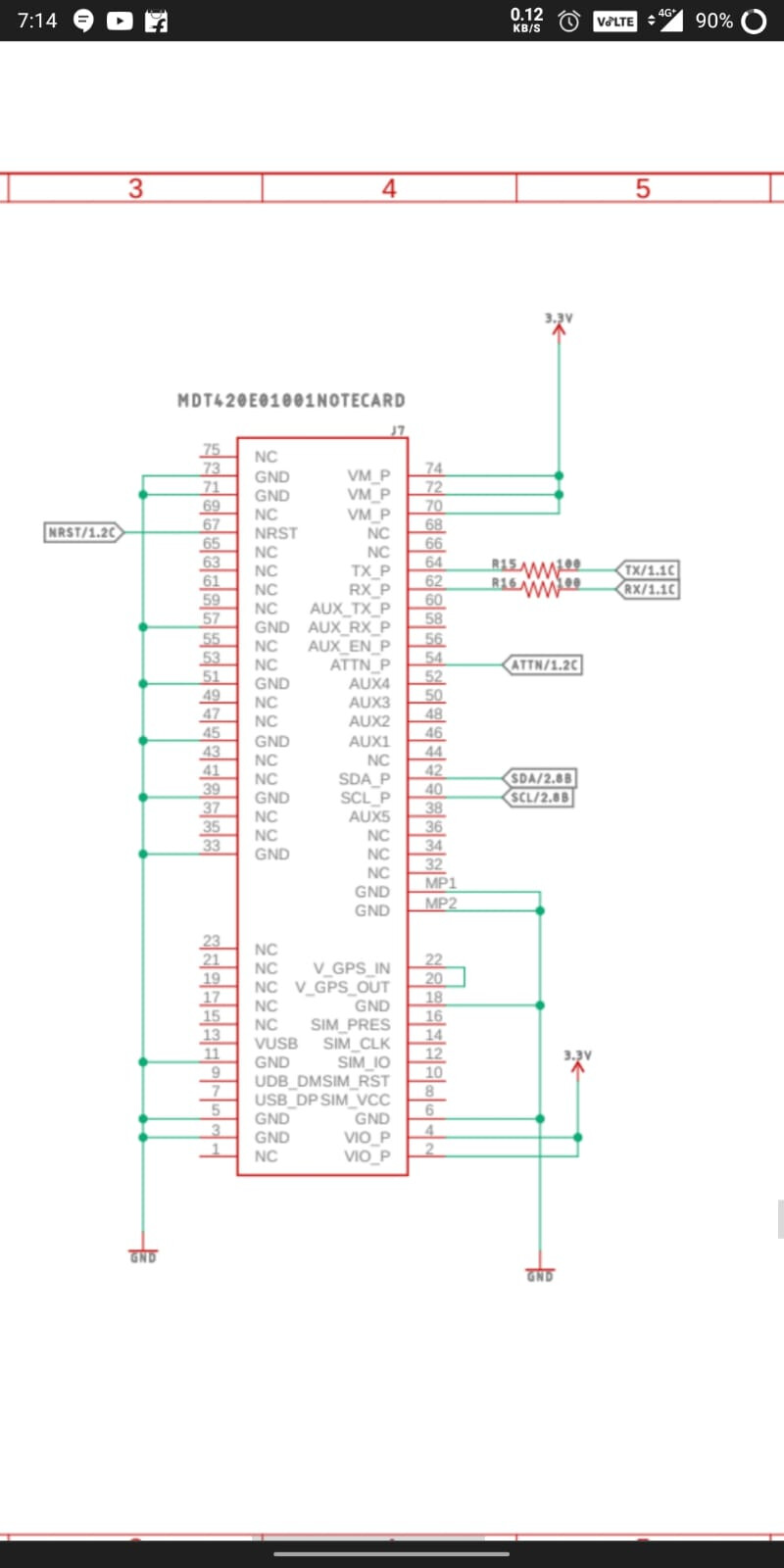
@Pradeep I’d like to start by apologizing for the delay. Your schematic looks good! ![]()
I looked for a bit and your additions are solid. You did a really great job! Thank you for noticing the discrepancy between designs because it allows me the opportunity to offer a better explanation for why that is, and why you shouldn’t deviate from your current approach.
NRST is an optional active-low Notecard input/output. However, when dealing with a scenario where a reset signal needs to be sent to multiple devices, it is crucial to take extra precautions to ensure that the Notecard does not accidentally reset other equipment (and visa versa). This is where the isolation of the reset signal using a transistor becomes your saving grace.
As you add more components to your system, having the reassurance that your device is reset precisely when intended becomes a sanity check. By implementing the reset pin isolation with a transistor, you provide a valuable safeguard for your design.
~VMODEM on the Notecard/ M.2 connector require a voltage range of +2.5VDC ~ +5.5VDC for safe and proper operation. The power supply should be capable of sustaining a draw of 750mA continuously and handling brief bursts of 2A. The purpose of a fuse on this line is to act as a safety device that interrupts the circuit if there is an overcurrent condition, preventing damage to the modem.
~USB_DP, USB_DM, VUSB, (and GND) provide an additional USB interface, utilizing the same JSON serial command/response protocol as the other serial interfaces. While your final design may not necessarily need this USB interface, it holds significant value, especially during the development phase. This USB interface is particularly useful during system development since it is supported by all operating systems. Additionally, although the Notecard operates with ultra-low power, having the option to power or recharge via USB can be convenient. On a slightly different note, the external SIM functionality follows a similar concept. Even if your final design does not require it, considering its inclusion can be advantageous.

ACT_GPS_OUT on the Notecard is specifically designed and intended to provide a regulated power supply for the LNA when GPS functionality is activated. It is pertinent that this you take special care of this port as other components or devices may require different voltage levels, and using VACT_GPS_OUT for unintended purposes may result in improper voltage levels that may damage to those components.
If additional components or devices are connected to this pin, they may draw excessive current, exceeding the intended capacity of VACT_GPS_OUT and causing potential voltage drops or even damaging the power supply circuitry.
Also note that using VACT_GPS_OUT for unintended purposes may introduce additional noise or interference onto the power supply line. If you have other components or devices that require power, it is advisable to use separate and appropriate power sources to avoid potential issues and ensure the optimal performance of the entire system. This ties back to my notes on Pin67
I’ll note that you may be interested in an alternative, lower-Iq (or price or availability) +3V3DC regulator for @ the LoRa device. The SX126 should only draw ~10mA in receive mode and ~100mA in transmit mode so right now you’re
Would you mind telling me a bit more about your design so I have a better idea of where your head is at? It may help me guide you in the right direction as quickly as possible. At the end of the day (especially with RF), your best bet is usually to follow our design guides as closely as possible. Even if it means not utilizing a particular component in a specific scenario, adhering closely to the design guides will help optimize RF functionality. However, if you have budget constraints or limited space, please feel free to elaborate on your thought process, and we will do our best to assist you.
If it’s on your Carrierboard and you don’t think you need it- just ask! Are you planning to design your own board(s)? If so, continue to follow the fundamental rules you have been using as you are already off to an excellent start! ![]()
Hi @twojo , First of all thank you so much for your time to give these answers and comments. Seriously these very helpful and I have dig more on some parts.
Here is my design details.
My plan is to build a custom Notecarrier board with external sim support which is directly connected to Xiao RP2040 controller via i2c. And in the same carrier board I’m planning to implement the LoRa E5 chip which is connected to the Xiao RP2040 via UART.
So finally I can receive data from Lora E5 and revert back to nothub via the Notecard.
Let me know if there is any questions.
Regards,
Pradeep S.